GPU Basics: What & Why
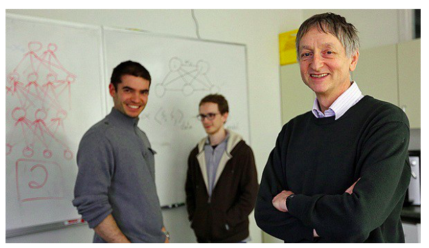
The SuperVision team: Alex Krizhevsky, Ilya Sutskever, and Geoffrey Hinton
The ImageNet competition was an annual contest where AI models competed to classify objects across millions of images. In 2012, it was dominated by teams running hand-engineered computer vision features on CPU clusters. Then team SuperVision from the University of Toronto mogged on the competition with AlexNet, a neural network trained on two $500 gaming cards. They posted a 15.3% error rate; the runner-up managed 26.2%. Previous winners had improved by fractions of a percent.
By this point, neural networks had gone through numerous “winters” and had been sidelined by the research community in favor of other classical ML algorithms. SuperVision’s revolutionary insight was that, given the right architecture, performance scaled with training, and GPUs could be used to make scale fast and cheap. Many refer to this as the “big bang” of modern AI.
Almost everything since, from GPT to Claude to Gemini, is downstream of that same bet. Since 2020, training compute for the frontier (top-5) language models has been been growing at ~5x per year.
Moreover, scaling laws have roughly kept up with this thesis. For now, more compute seems to translate into predictable performance gains.
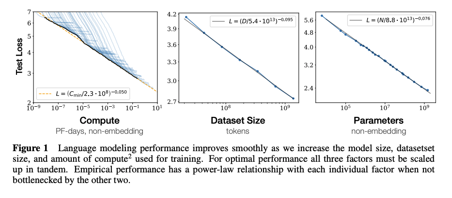
Therefore, its important to recognize that the hardware that AI runs on is as important of an input as the architectures themselves. The two are tightly interlinked and, with the rise of custom silicon, this dependance will likely only increase. You can’t build efficient ML systems without a good mental model of GPUs and that is what this post aims to bolster: What is a GPU? Why do they work so well for AI? What are the trade-offs?
Most of this material is from my digest of [Stanford CS336 (https://github.com/stanford-cs336/)] by Tatsu Hashimoto, plus extra context. For those with ample time, I highly recommend the entire course. This post is meant to be pedagogical and the start of a series on GPUs and LLMs.
So why did we need GPUs at all? Because around 2005, chips stopped getting faster from traditional methods.
Dennard vs Parallel Scaling
From the 1980s to the mid-2000s, compute scaling relied on Dennard Scaling: shrinking transistors let them run at a lower voltage, increasing clock speed for free.
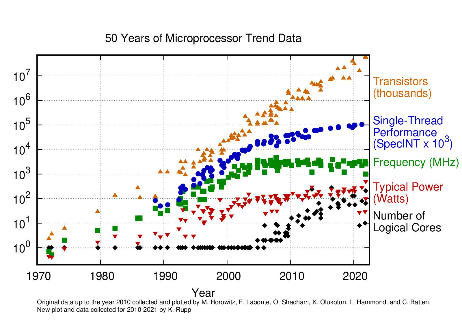
Unfortunately, this broke down around 2005. While Moore’s Law continued, voltage hit a floor at ~1V. Below this threshold, transistors never fully switch off, and the wasted power grows exponentially. With voltage frozen, raising clock speed meant more power and more heat than a chip could shed, so clocks stalled at 3–4 GHz.
Aside: Each chip has an oscillator cycling at some clock speed of N ticks per second (e.g., 3 GHz = 3 billion ticks/cycles). Each tick advances the entire chip in lock-step. Roughly speaking, cranking up a chip’s clock speed makes it complete the same work proportionally faster.
Dynamic power is P ≈ C·V²·f (capacitance × voltage² × frequency), measured in Watts. As each individual transistor took less voltage, the same amount of power allowed for much greater clock speed (increased frequency).
Increasing clock speed alone means greater power demand and therefore more heat. At greater temperatures, the chip ages faster and transistors begin to slow or fail. To mitigate, temperature sensors within the chip trigger “throttling”. That is, the chip decreases its clock speed to make room for slower transistor speed and protect it from crashing.
With continually increasing transistor counts, a new paradigm of parallel scaling emerged. If you can’t increase the speed, just use the transistors to do more work concurrently. Core count began increasing, and GPUs took this to the extreme. In 10 years, GPU throughput rose 1000x while single-thread CPU performance inched. So how exactly do GPUs leverage this paradigm?
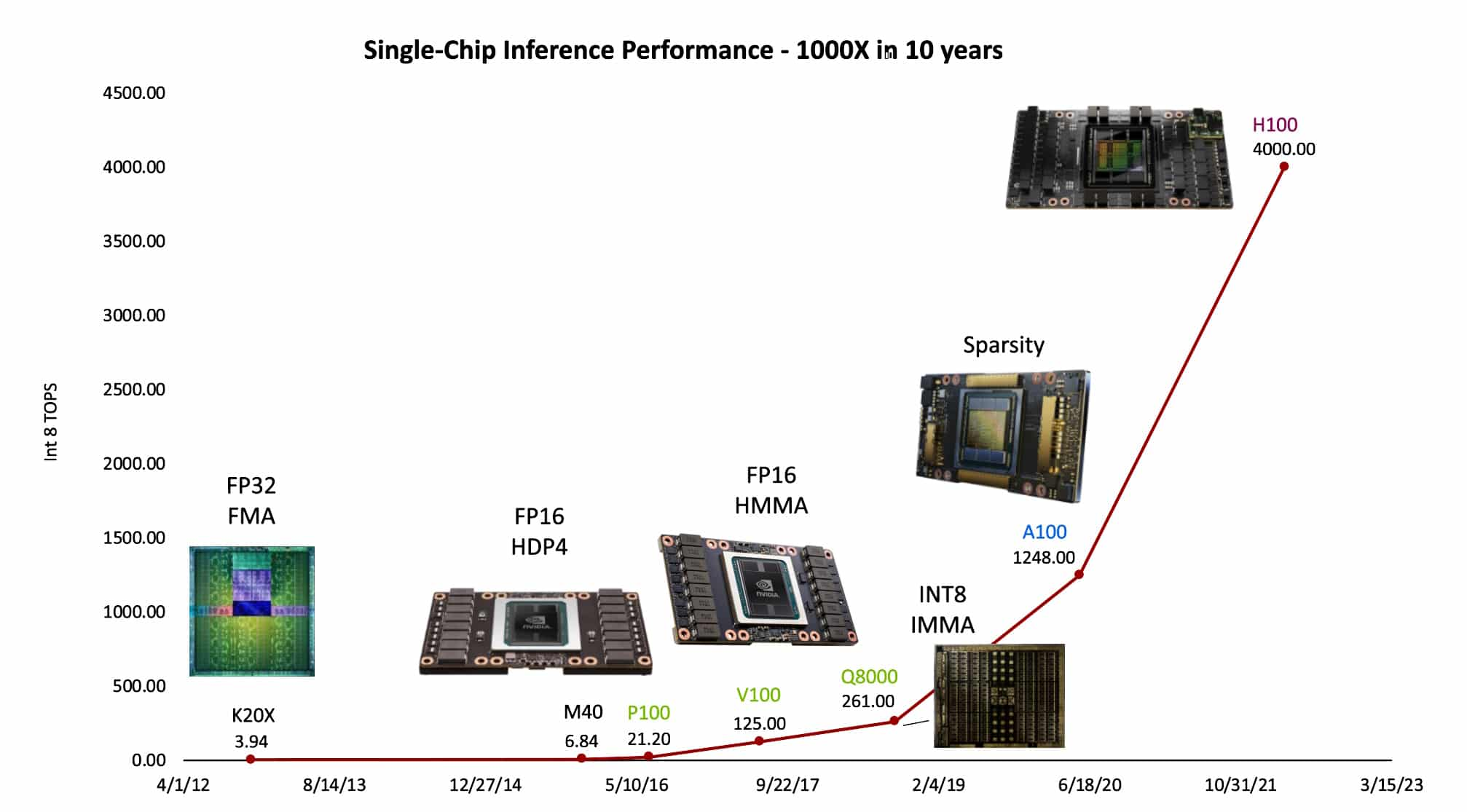
- [fig: Bill Dally, “Trends in Deep Learning Hardware”, Hot Chips 2023 keynote]
CPUs vs GPUs
At the core, the trade-off is latency versus throughput. CPUs excel at running a few fast threads; GPUs run thousands of slow ones.
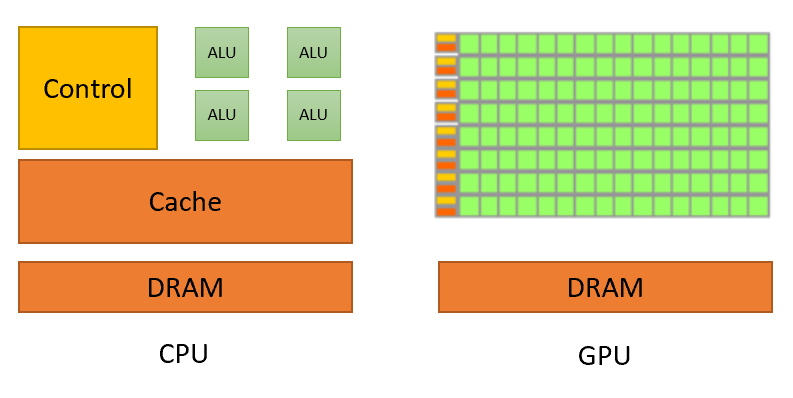
[https://developer.nvidia.com/blog/cuda-refresher-reviewing-the-origins-of-gpu-computing/]
This is visible on the silicon itself. A CPU spends a huge amount of its transistor budget on control: branch prediction, big caches, out-of-order execution. Lots of machinery to make extremely fast and flexible threads. On the other hand, a GPU spends most of its budget on ALUs (Arithmetic Logic Units). An ALU, as the name suggests, is the circuit that actually executes operations on values: arithmetic, logic, comparisons. Strictly, floating-point math and other complex operations live in their own units, but “ALU” is often used loosely to contain any of these execution circuits. Unsurprisingly, you’ll find that GPUs are terrible at branchy, sequential logic and CPUs are wasteful at bulk arithmetic.
It’s also worth noting that modern CPUs did adopt some of this paradigm shift as well. In 2005, Intel and AMD shipped their first dual-core processors (Pentium D, Athlon 64 X2). In 2025, AMD EPYC tops out at 192 cores — roughly trailing Moore’s law at ~2x every 2.5 years.
So what’s inside a GPU that allows it to optimize for throughput?
Basic Anatomy of a GPU
A lot depends on the make/model, so the following will be a look at the Tesla V100, NVIDIA’s data-center GPU based on the Volta architecture, released in 2017.
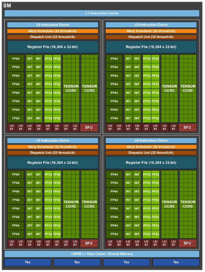
A V100 SM
A GPU is built from SMs (Streaming Multiprocessors) that independently execute blocks. Each SM includes many execution units, chiefly SPs (Streaming Processors), the FP32 lanes that NVIDIA later rebranded as CUDA Cores. These execute threads in parallel.
A thread is simply a stream of instructions and data assigned to a SP. A block, or thread block, is a collection of up to 1,024 threads assigned to run on a single SM. A block can never be split across SMs, which is what lets its threads cooperate and share memory. A warp is a collection of 32 threads that execute in lock-step, controlled by the warp scheduler.
Zooming into the V100 SM, it’s divided into four identical quadrants, each a self-contained execution engine.
At the top of each quadrant: an L0 instruction cache feeding a warp scheduler paired with a dispatch unit, both rated at 32 thread/clk, i.e., 32 threads served per clock cycle. The scheduler picks which warp goes next; the dispatch unit routes that instruction to the right pipeline. Below sits a 16,384-entry register file.
Then the compute lanes: 16 FP32 cores, 16 INT cores, 8 FP64 cores, and 2 Tensor Cores per quadrant. The INT and FP32 pipelines are physically separate, so loop index math and floating-point math run concurrently. Transcendental functions (sin, cos, sqrt) get routed to a dedicated SFU (Special Function Unit) rather than burdening the SPs. The two Tensor Cores, new with Volta, are matmul macro-units: instead of one value per lane, each consumes an entire warp’s data to perform a small matrix multiply-accumulate per clock, making them >10x faster than the FP32 lanes for this workload.
Finally, eight LD/ST (load/store) units per quadrant handle memory traffic, computing addresses and moving data between registers and the memory hierarchy, so memory ops and arithmetic overlap.
Note the mismatch: warps are 32 threads but a quadrant has only 16 FP32 lanes, so an FP32 instruction actually issues over two cycles, pipelined through in halves. And since the pipelines are independent, the scheduler can issue an FP32 op one cycle, an INT op the next, an FP64 op after that, and all three pipes churn concurrently on different warps.
For reference, a V100 has 80 SMs with 64 FP32 SPs each, for 5,120 CUDA cores total. Before Tensor Cores existed, researchers would hack programmable shaders, meant for rendering graphics, to do matmuls.
Memory Hierarchy
The other half of the chip is dedicated to memory. In general, the closer the memory to the computation, the faster.
Per-thread registers and shared memory/L1 live inside each SM. L2 sits on the die, shared by all SMs. Global memory, i.e., High Bandwidth Memory (HBM), is stacked DRAM sitting next to the die, and it’s the largest and slowest tier by far.
For the V100, roughly:
| Tier | Size | Latency (cycles) | Bandwidth |
|---|---|---|---|
| Registers | 256 KB per SM | ~1 | ~20 TB/s effective |
| Shared / L1 | 128 KB per SM | ~30 | ~14 TB/s |
| L2 | 6 MB | ~200 | ~2–3 TB/s |
| HBM2 | 16–32 GB | ~400–600 | 900 GB/s |
How the flagship datacenter GPUs have evolved:
| V100 (2017) | A100 (2020) | H100 (2022) | B100 (2024) | Rubin (2026) | |
|---|---|---|---|---|---|
| SMs | 80 | 108 | 132 | 160 (2 dies) | 224 (2 dies) |
| CUDA cores | 5,120 | 6,912 | 16,896 | 20,480 | TBD |
| Tensor FP16/BF16 (dense) | 125 TFLOPS | 312 TFLOPS | ~990 TFLOPS | ~1,750 TFLOPS | ~8,000 TFLOPS* |
| HBM | 16–32 GB, 900 GB/s | 40–80 GB, ~2 TB/s | 80 GB, ~3.35 TB/s | 192 GB, ~8 TB/s | 288 GB HBM4, ~22 TB/s |
(Blackwell hit TSMC’s reticle limit, so it fuses two dies into one logical GPU; 160 SMs is the full configuration, with shipping parts enabling slightly fewer.) Notice the asymmetry: from V100 to B100, compute grew ~14x but memory bandwidth grew only ~9x, and the gap was even starker at the H100 (~8x vs ~3.7x).
A tool fit for its task
Why does this architecture fit neural networks so well? Because nearly everything a neural net does is data-parallel: the same operation applied independently across multi-dimensional arrays called tensors. This was the insight the SuperVision team understood, and what allowed neural networks to pull ahead from classical machine learning algorithms.
In 2012, Alex Krizhevsky hand-wrote CUDA kernels to run them across two GTX 580 and trained a network too big for any CPU cluster of comparable cost. Today, NVIDIA is the largest company in the world with a valuation north of 4.5T USD, in-part due to that same bet.